Description:
Market Opportunity
The need for high-speed, medium-resolution analog-to-digital converters (ADCs) is rapidly growing due to the increasing demand for wideband communication integrated circuits. The traditional voltage-domain time- interleaved SAR time-to-digital converter (TDC) is an efficient option, but its single-channel sample rate is limited, necessitating a large number of TI channels. Recently, time-domain ADCs have shown promise in high- speed scenarios, but their circuit complexity grows exponentially with the target bit resolution.
USC Solution
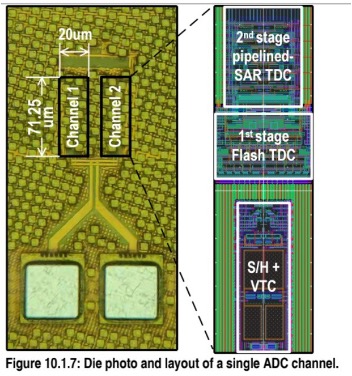
USC inventors have developed a two-step time-domain ADC that reduces size, cost, and circuit complexity. The technology uses a first-stage Flash TDC with residue time quantized by second-stage SAR TDC to target the >GS/s regime and address the limitations of existing solutions. A proof-of-concept ADC prototype using this technology reaches 10GS/s with 37.2dB SNDR at Nyquist frequency while measuring an energy efficiency of 24.8fJ/conv-step. The device takes up an active area of 2850um2, the highest reported energy efficiency and smallest area consumption for state-of-the-art ADCs with greater than 10GS/s.
Value Proposition
Applications
Publications
A 10GS/s 8b 25fJ/c-s 2850um2 Two-Step Time-Domain ADC Using Delay-Tracking Pipelined-SAR TDC with 500fs Time Step in 14nm CMOS Technology, Liu et al., 2022.
Stage of Development